My etched PCB process works, but it is a lot of steps and a lot of chemicals, and the holes still have to be drilled by hand at the end. Now that the CNC machine has a Dremel sled and working endstops, I have been trying the other way of making a board at home: put a copper blank on the bed and let a V-bit cut the copper away between the traces. No photoresist, no artwork, no developer, no ferric chloride, and the machine drills the holes in exactly the right place because it is the same file that cut the traces.
This is the short version of the process. The boards come off the machine as bare copper: no immersion tin, no solder mask, no silkscreen. They are milled, drilled, cut out and soldered as they are. That is all a board with a handful of through-hole parts needs, and the full version with tin and a machine-opened solder mask is a separate post once I have it working. The board in the photos is the same ESP32-C3 button board as the etched post, redrawn with fatter traces and a ground pour.
Why mill instead of etch
| Etch | Mill | |
|---|---|---|
| Chemicals | Developer, ferric chloride, acetone, tin | None |
| Artwork | Print, mirror, double, glue, align | None, the G-code is the artwork |
| Resolution | Limited by the acetate and exposure | Limited by the V-bit tip, runout and board flatness |
| Holes | By hand with a pin vice | Machined, in the right place |
| Time per board | Mostly waiting on chemicals | Mostly machine time |
| What goes wrong | Over or under exposure, light leaks, over-etch | Board not flat, bit too deep, lost zero |
Milling makes the most sense for boards with a few parts and generous spacing. The V-bit in the Dremel cuts a slot about 0.5 mm wide, so anything fine-pitch or dense is still better etched, or ordered. For a breakout board with some headers and a button it is ideal.
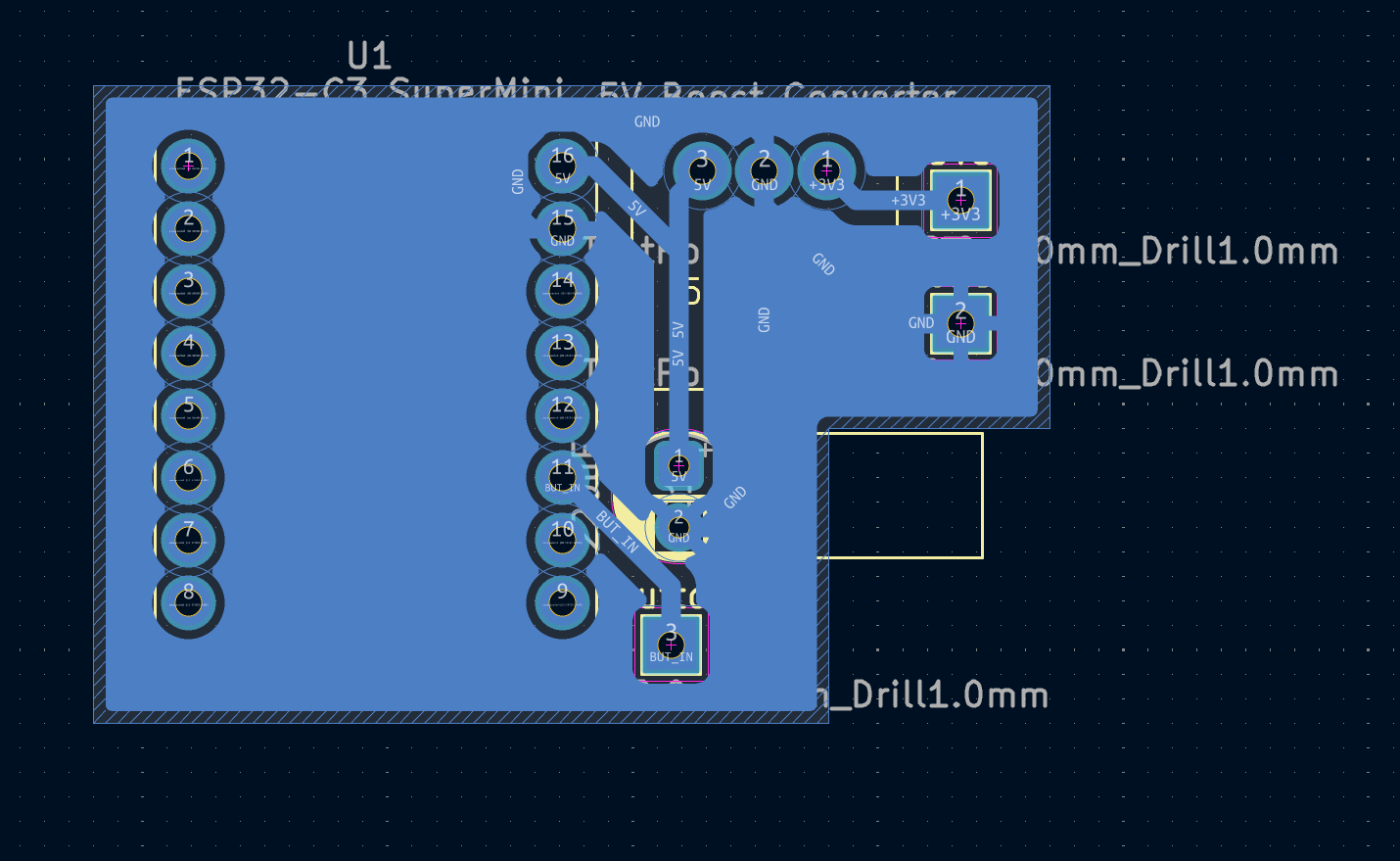
1. Design in KiCad, for a V-bit
The layout is a normal single-sided through-hole design with the copper on B.Cu, but the design rules have to be set up for the cutter rather than for a fab house. The one number everything hangs off is the real width of the slot the bit cuts, which on this machine is 0.5 mm (the bit's geometry plus the Dremel's runout, measured on scrap rather than calculated). The isolation pass has to fit at least one full slot between every pair of copper features, and if the KiCad clearance is smaller than that FlatCAM silently skips the gap and the two features stay shorted. So: minimum clearance 0.6 mm, track width 0.5 mm or wider, annular ring 0.6 mm, holes 0.7 mm, copper-to-edge 1.0 mm. Pads get fattened to 2.2 mm or more, because the standard 1.6 mm pad on a 0.8 mm hole leaves a 0.4 mm ring and the kerf and the drill between them will remove it.
The other thing that makes a big difference is a ground pour on B.Cu. Without one the machine has to clear every square millimetre of unused copper, which takes forever and leaves the board rough. With one, the isolation pass only cuts a thin line around each trace and pad and the rest of the copper just stays there as ground. Thermal reliefs on the GND pads (0.5 mm gap, 0.6 mm spokes) keep them solderable; solid connections sink too much heat. Finally the drill/place origin goes on the bottom-left corner of the board outline, because that is where the machine's work zero will be.
2. Gerbers to G-code in FlatCAM
KiCad plots B.Cu and Edge.Cuts as Gerbers and the holes as an Excellon file, all using the drill/place origin. Those go into FlatCAM, which is abandoned software that nobody has replaced: the official site still offers a version from 2016, the Beta branch everyone actually uses stopped getting releases years ago, and there is no working Windows installer any more. It runs from source inside a conda environment built from the environment.yml it ships with, which is a faff once and fine after that. It is still the only free tool that does isolation routing, drilling and the outline in one place.
The first thing to do in FlatCAM is mirror everything. B.Cu is milled with the copper facing up, so the whole job is mirrored about the outline, every object once, and then the origin is put back on the bottom-left corner. Then three kinds of file come out of it:
- isolation.nc, from the Isolation Routing tool on B.Cu. Tool type C1 (plain circular, so it doesn't recompute the width from the bit angle), diameter 0.5 mm, one pass, climb milling. Cut Z -0.10, travel Z 2.0, feed 200 mm/min, plunge 50 mm/min.
- drill-0.8.nc, drill-1.0.nc, one per drill size from the Drilling tool, because GRBL errors on the
M6tool change it would otherwise put between them. Cut Z -1.8 (through a 1.6 mm board and into the spoilboard), plunge 60 mm/min. - cutout.nc, from the Cutout tool on Edge.Cuts. 1 mm end mill, -1.8 in 0.5 mm steps, four 3 mm tabs so the board doesn't come loose and get flung on the last pass.
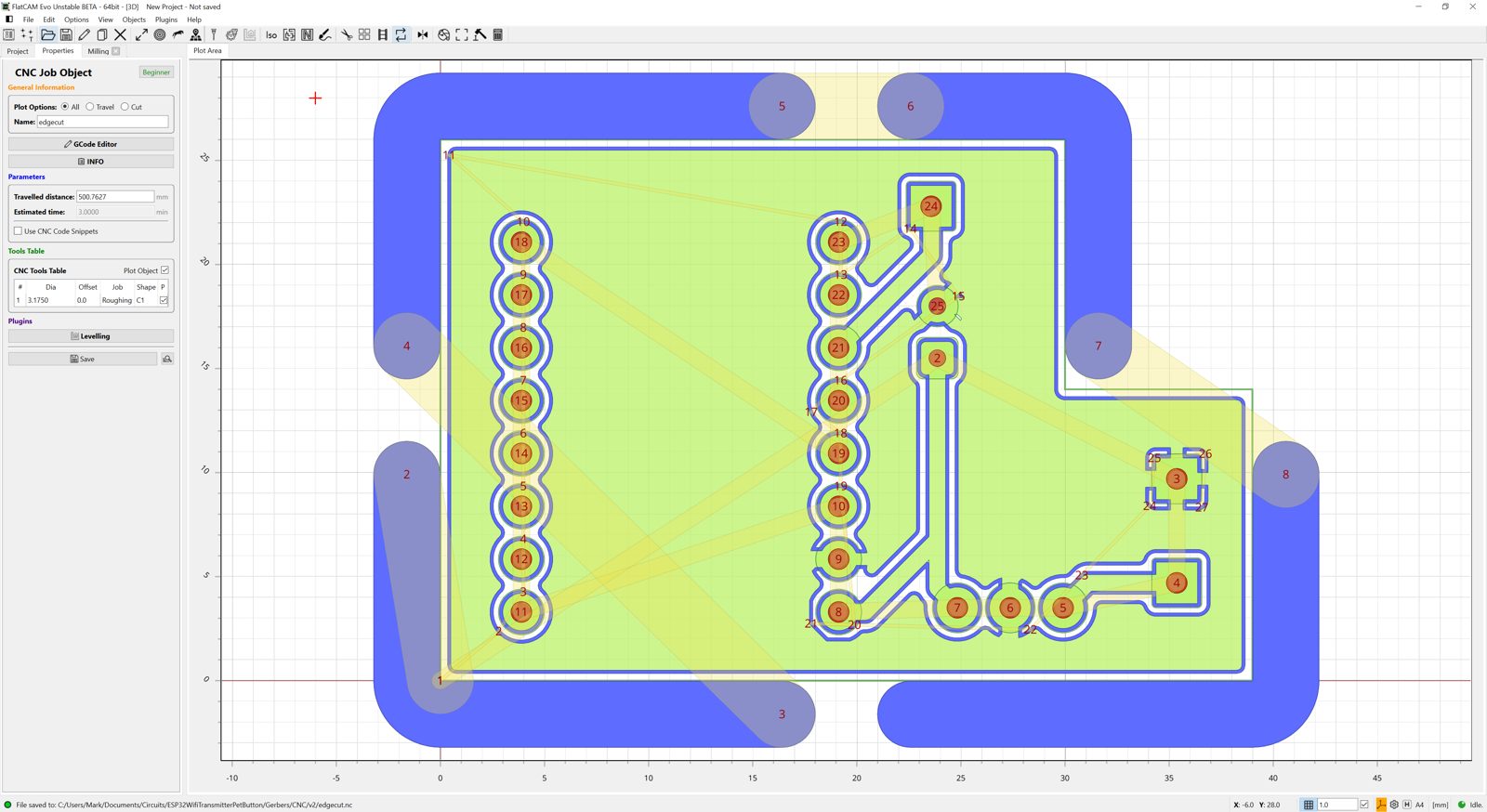
That is what the project looks like with everything generated: the thin outlines hugging the traces are the isolation, the numbered dots are the drills, the wide band is the cutout. The check before saving anything is that the drill dots sit in the middle of the pads. If they are all offset the same way, the mirror was done on some objects and not others.
The tool diameter is the setting that cost me the most boards. FlatCAM puts the centre of the slot half a diameter away from the copper edge, so if the diameter is smaller than the real kerf the slot overlaps the copper and every trace comes out thinner than designed. My first attempts used two passes at a diameter of 0.15 mm, which is roughly what the V-bit angle predicts and about a third of what it actually cuts:
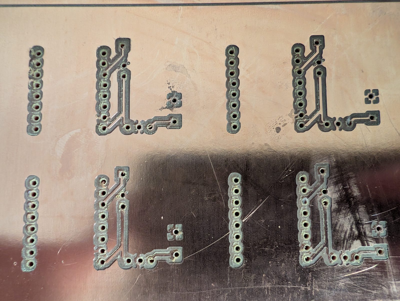
Wide slots, traces half their width, and the drill pulled what was left of several pad rings clean off. The fix is to measure the slot on scrap with a loupe and rule, set the diameter to that, use one pass, and get any extra clearance from the KiCad rule rather than a second pass. If anything, err 0.05 mm large: the sliver that leaves is attached to the trace and just makes it a little wider.
3. Fixture the blank and set the zero
The blank is stuck to a surfaced spoilboard with thin double-sided tape (carpet tape, not foam) and pushed hard into a corner fence of two MDF strips glued down at right angles. The fence is what makes it possible to take the board off and put it back in the same place later. The machine is homed first so every position is repeatable, then the 30° V-bit goes in the Dremel, short in the collet, and gets jogged until the tip is over the corner of the blank. The board outline sits 5 mm in from the blank corner, so the zero is set with G10 L20 P1 X-5 Y-5, which tells GRBL the bit is currently at X-5 Y-5 and puts work zero exactly on the board corner. I write down the machine position from ? at this point so the zero can be recovered if anything goes wrong.
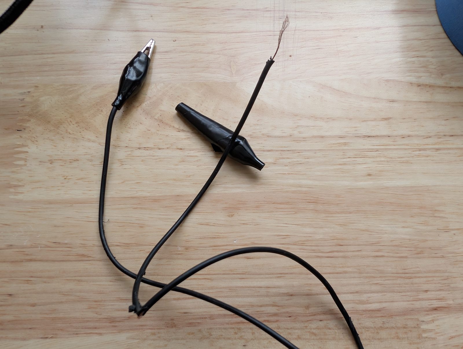
Z is not set by eye. A crocodile clip on the copper and another on the bit go to the probe pin on the CNC Shield, and G38.2 Z-5 F30 brings the bit down until it touches. That is how the lead in the photo below died. I finished probing, forgot the clip was still hanging off the shank of the bit, and switched the Dremel on. The clip went round with the bit, the wire wrapped itself round the shank in a turn or two, and at 30,000 rpm it was yanked straight out of the crimp before I could reach the switch. So, both clips come off before the Dremel is started: the one on the bit because it will be flung off and take the wire with it, and the one on the copper because the lead is then lying across the board in the path of the cut. Take them off as the last thing after probing, every time, and solder the wires into the clips while you are at it rather than trusting the crimp.
4. Probe a height map
This is the step that makes or breaks the whole thing. The cut is 0.1 mm deep, and copper clad is never flat to 0.1 mm: a few tenths of bow across a blank is normal, which is several times the depth of cut. Zero the bit in the middle and run the file without correcting for that and this is what happens:
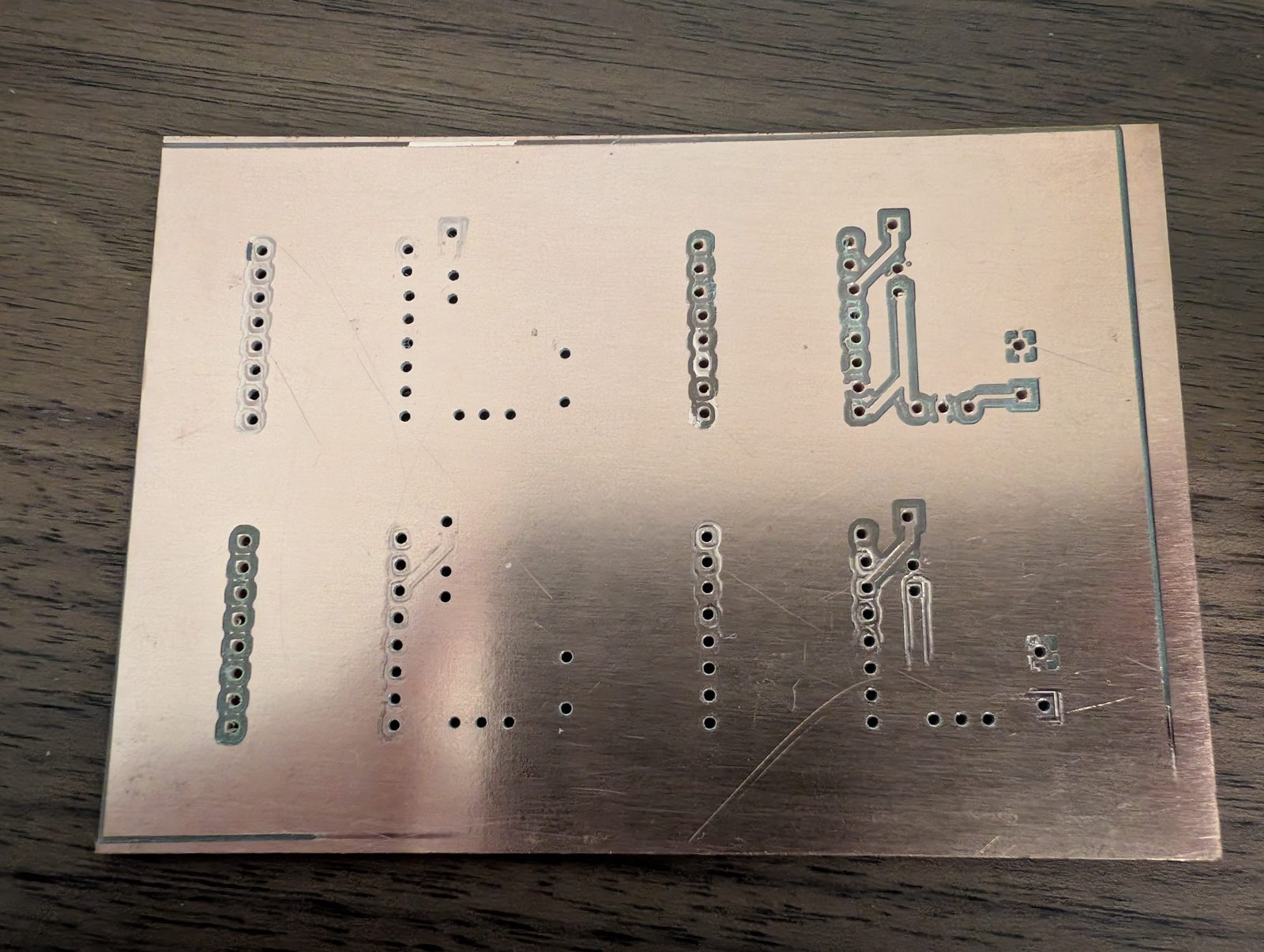
Same file, same Z zero. On one side of the panel the traces are fully isolated; on the other the bit skated over the copper and only the drills went in. The fix is the AutoLeveler plugin in Universal Gcode Sender Platform (it only exists in the Platform version, not Classic). With the probe clips still on, it probes a grid of points across the board, 10 mm apart, and then rewrites every Z in the loaded G-code to follow the measured surface.
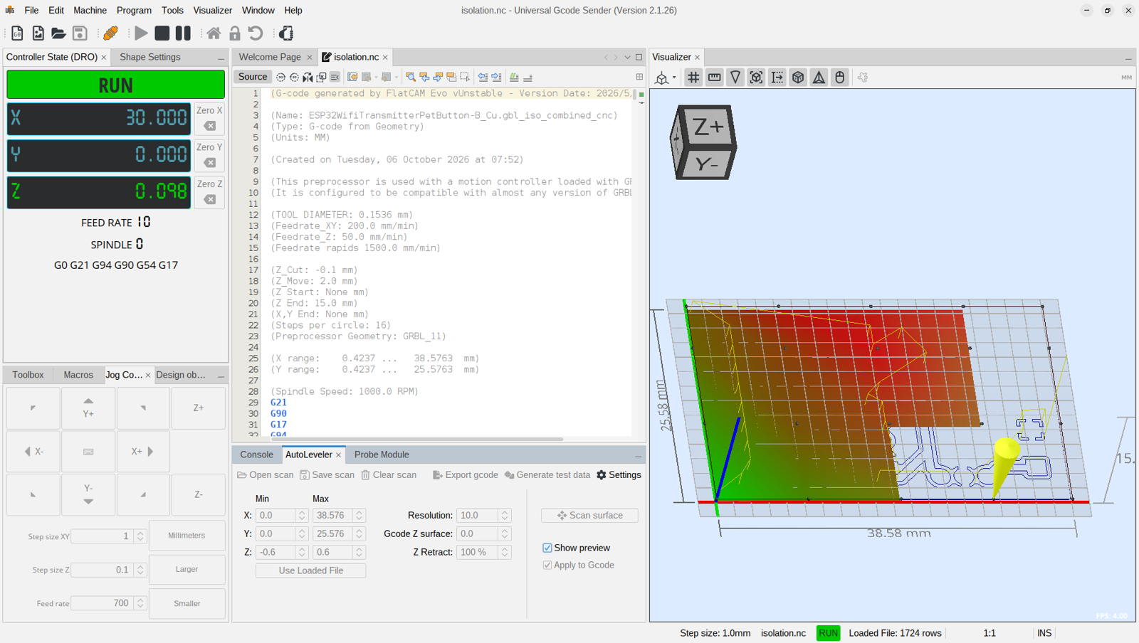
The colours are the point: this blank varies by a few tenths of a millimetre across 40 mm. The scan gets saved with the job so the drill and cutout files can have the same map applied without probing again. If the map shows more than about 0.3 mm of variation the blank isn't stuck down flat, and the answer is to pull it up and redo the tape rather than let the map paper over it.
5. Mill, drill, cut out
Both probe clips off, dust mask on, vacuum nozzle by the bit, Dremel on its top speed (small V-bits want all the rpm they can get), and run isolation.nc. The first few cuts tell you whether the depth is right: you want a clean shiny line with the copper fully gone and only a faint scratch in the fibreglass underneath. If the bit is skating, stop, drop the Z zero by 0.02 mm, re-apply the height map and go again; if it is throwing white dust it is too deep and goes the other way. I don't walk away from the first board, because if the bit is going to break it does it on a plunge.
When it finishes the board stays where it is and gets a look under a magnifier for any isolation line that hasn't gone all the way through; those can be re-run 0.02 mm lower while the zero is still good. Then the drills: swap in the 0.8 mm carbide drill, re-probe Z, run the 0.8 file, repeat for the 1.0 mm. Carbide PCB drills snap if the board moves at all, which is where the tape earns its keep. Finally the 1 mm end mill, re-probe, and the cutout file, or for a plain rectangle just a knife along the outline and snap it. Snap the tabs, file the edges, blow the dust out of the holes.
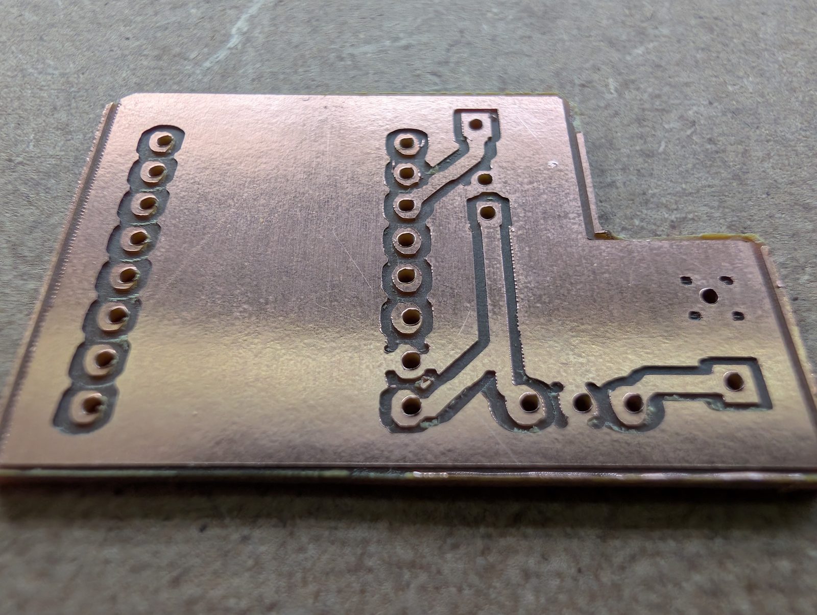
The first one that came out right. Clean 0.5 mm slots, full-width traces, every pad ring intact after drilling, and the ground pour left as one big piece of copper. Milled, drilled and cut out in one sitting, and soldered as it is.
Quick reference
| Operation | Tool | Feed / plunge | Cut Z | Notes |
|---|---|---|---|---|
| Isolation | 30° V-bit, 0.1 mm tip | 200 / 50 mm/min | -0.10 mm | FlatCAM tool C1, dia 0.5 (measured kerf), 1 pass, height-mapped |
| Drill | 0.8 / 1.0 mm carbide | – / 60 mm/min | -1.8 mm | One file per diameter, re-probe Z per drill |
| Cutout | 1 mm end mill | 150 / 50 mm/min | -1.8 mm in 0.5 steps | 4 tabs |
| KiCad rules | Clearance 0.6, track 0.5, annular 0.6, hole 0.7, edge 1.0 mm; pads 2.2 mm or more |
|---|---|
| Ground pour | Clearance 0.7, min width 0.5, thermal reliefs with 0.6 mm spokes |
| Spindle | Dremel 8220 at full speed, bit 10–12 mm out of the collet |
| Zero | Home, then G10 L20 P1 X-5 Y-5 over the blank corner |
| Probe | G38.2 Z-5 F30 then G10 L20 P1 Z0 |
| Height map | UGS Platform AutoLeveler, 10 mm grid, 2–3 mm margin |
| Before the spindle goes on | Both probe clips off, every time |
The three rules from this one: set the FlatCAM diameter to the kerf you measured, not the one the bit angle promises; never run the isolation pass without a height map; and keep the KiCad clearance bigger than the tool. The things I would like to add next are immersion tin so the copper stays solderable, and a solder mask with the pad windows opened by the machine from the same zero, which is the part that removes the last bit of artwork alignment from the whole process.