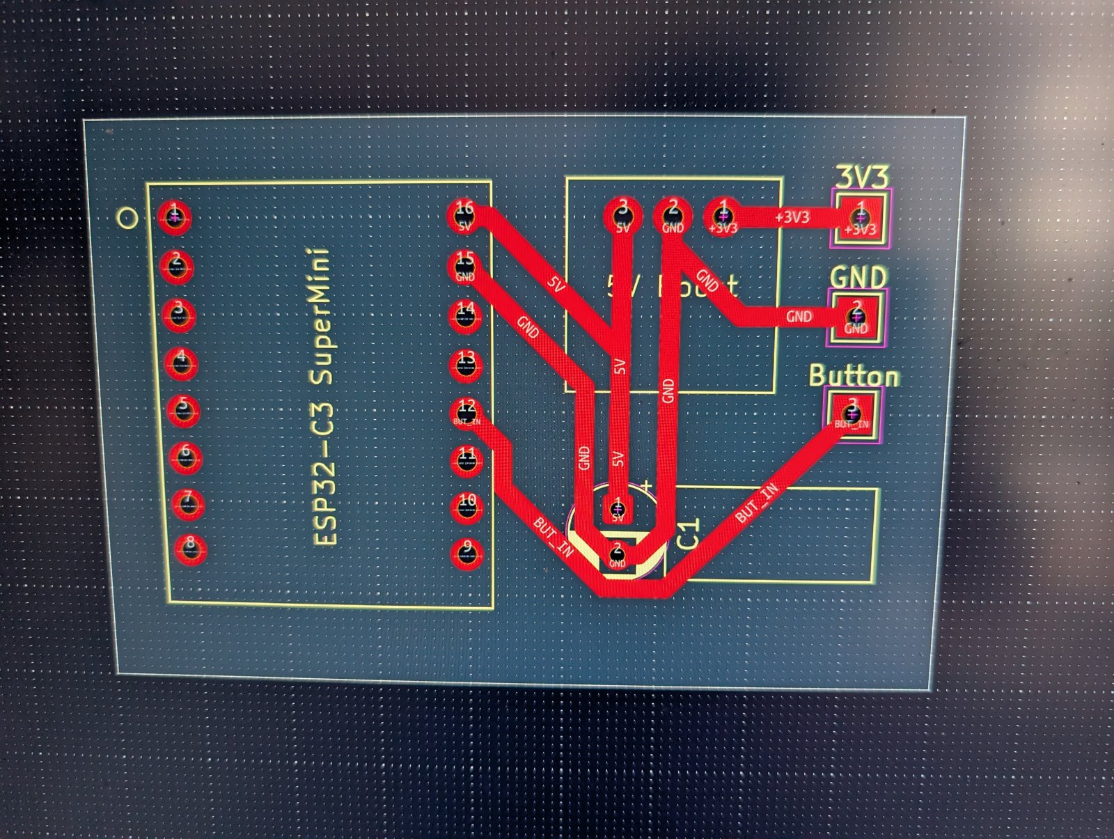
I have been making my own single-sided PCBs at home with dry film photoresist, a UV nail lamp and ferric chloride, and finishing them with immersion tin and a proper UV-cured solder mask. The process has settled down enough that I made a one-page poster of it for the workshop wall, so this post is the long version: what each step is, what it looks like, and the things that went wrong until I got them right. The board in the photos is a small ESP32-C3 SuperMini breakout with a button, panelised four to a blank.
The whole thing in one line: design, print the artwork, laminate on the film, expose, develop, etch, strip, tin, then do the film-expose-develop cycle a second time for the solder mask. Eleven steps, most of them minutes long.
1. Design in KiCad
The board is laid out in KiCad like any other. Because the blanks are bigger than the boards I usually want, I panelise several copies onto one blank so each run of the process produces a few boards instead of one. Single-sided, with traces kept a little wider than I would use for a fab house, since the resolution of a home process is limited by the printer and the film rather than by the etchant.
2. Print the acetate artwork
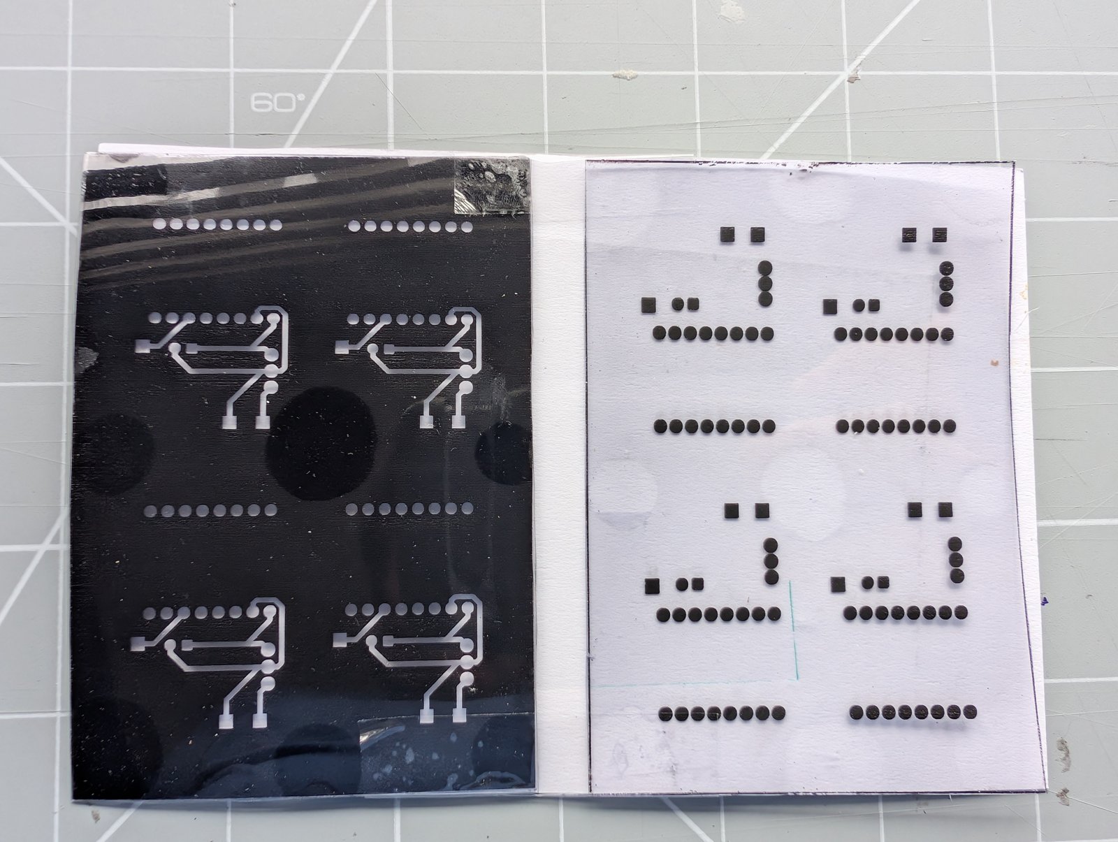
The artwork is printed to PDF with only the copper layer enabled, then printed onto acetate. Two things matter here. First, it has to be mirrored, so that when the acetate is laid on the board the ink side is not against the film: the printed side faces away from the board so the toner cannot smudge onto it and the image is the right way round on the copper. Second, a single sheet of toner is not opaque enough. Light leaks through and partially exposes the areas that should stay clear, so I print the artwork twice and glue the two sheets together, aligned, to block the stray light. A drop of alcohol on the non-ink side pulls the sheets into close contact so the double layer behaves like one dense mask.
3. Clean the board and apply the dry film
The copper has to be clean for the film to stick, so the blank is scrubbed first. The dry film photoresist comes as a sandwich with a protective backing on each side. Peel the backing off one side, press down one edge only of the film onto the board, and feed the board edge-first into a laminator. The laminator's heated rollers bond the film and push the air out ahead of them as the board goes through. Pressing the whole sheet down by hand before laminating traps bubbles, which become pinholes in the resist later, which become breaks in the traces; one edge, then the laminator, is the reliable way.
4. UV expose for 10 seconds
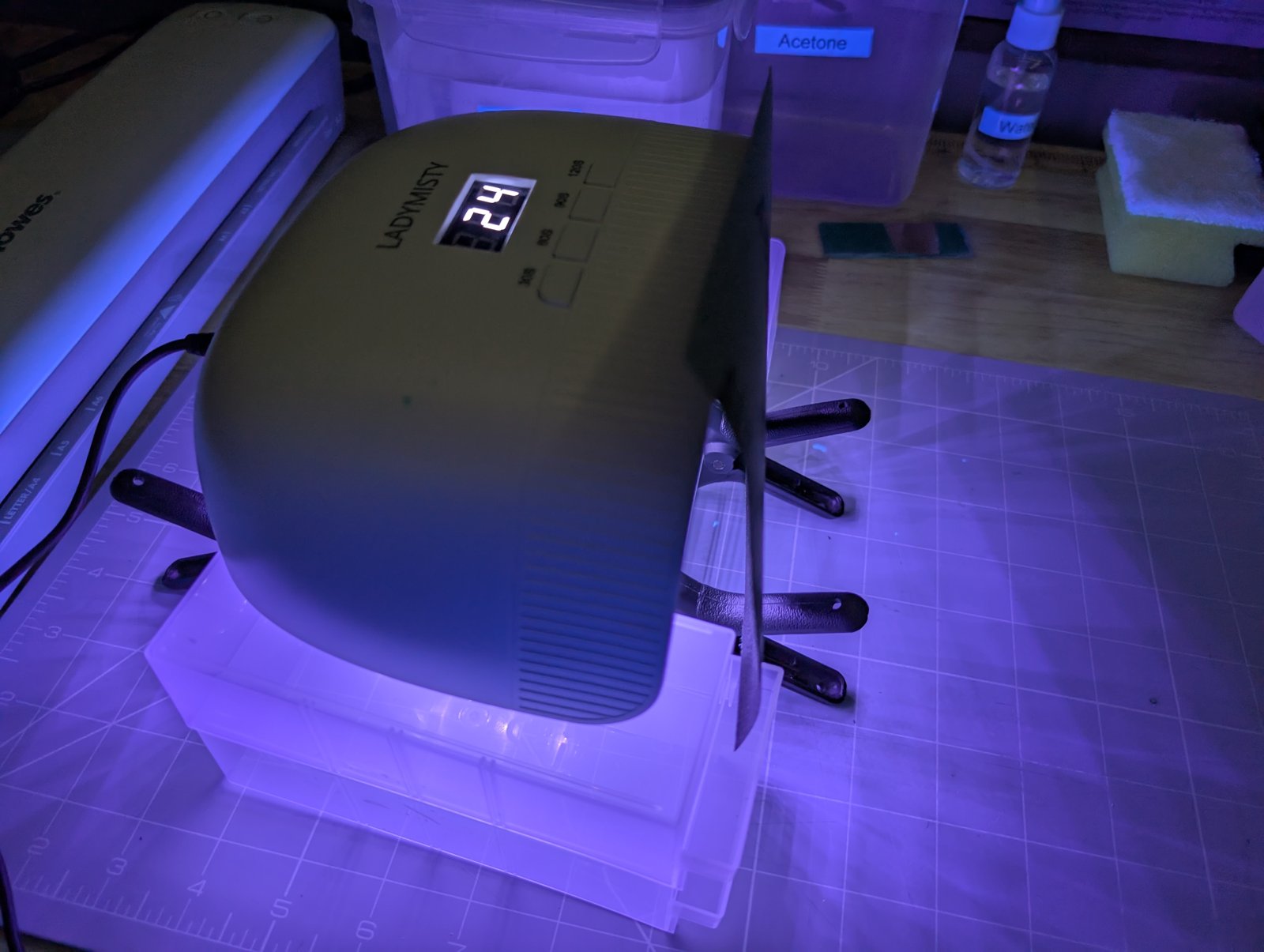
The artwork goes on top of the film and the board goes under a UV nail lamp for 10 seconds. That is not a typo. The lamp is far stronger than the film needs, and I tested exposure times from a few seconds up to a minute before settling on it; longer exposures bleed under the edges of the artwork and fatten the traces, and the clear areas start to cure too. The lamp has a timer, which takes the guesswork out of it.
5. Peel the cover sheet
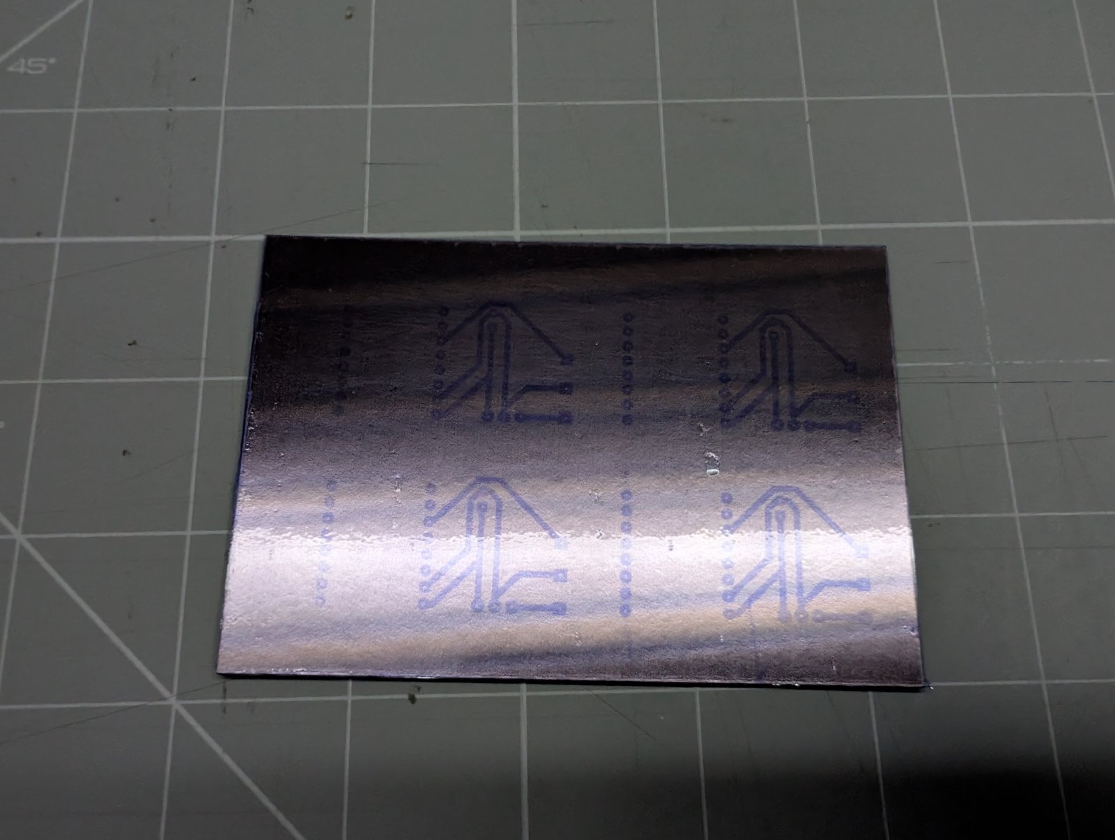
After exposure the latent image is already faintly visible in the film: the exposed areas have cured and changed colour slightly, so the traces show as a shadow of the artwork. The second protective plastic layer is still on at this point and has to come off before developing, otherwise the developer never reaches the resist.
6. Develop and re-cure
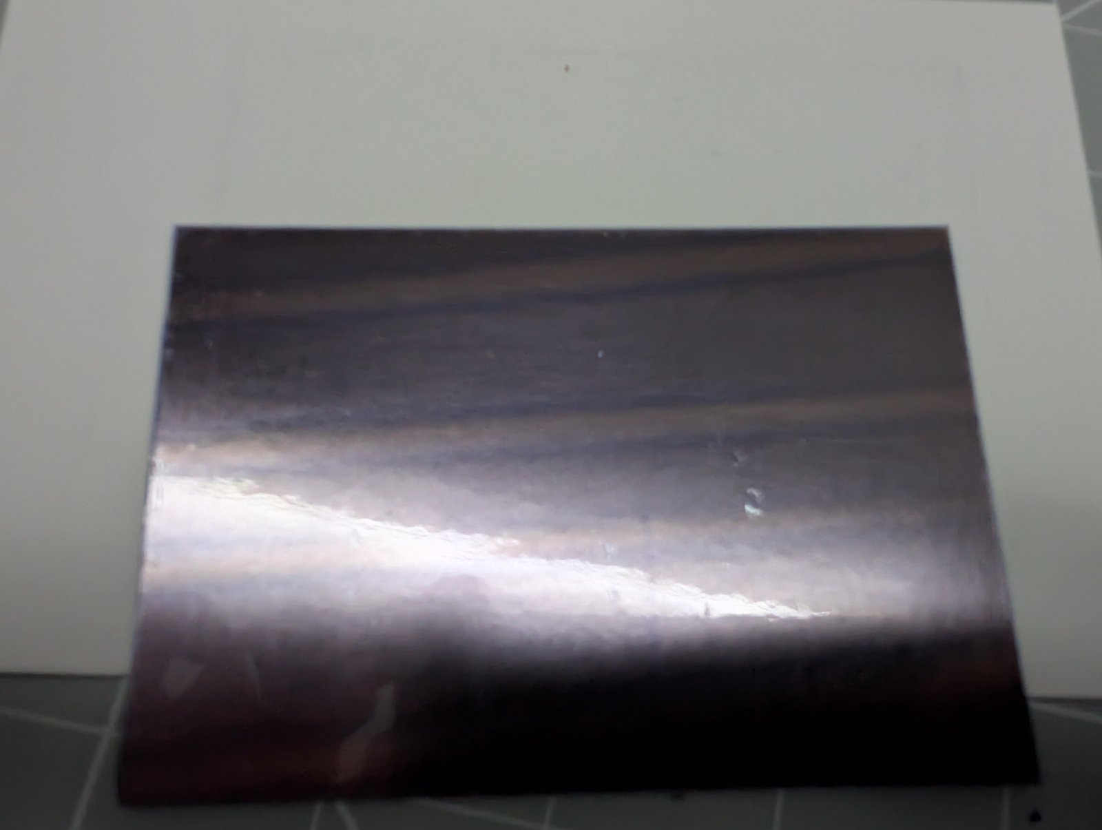
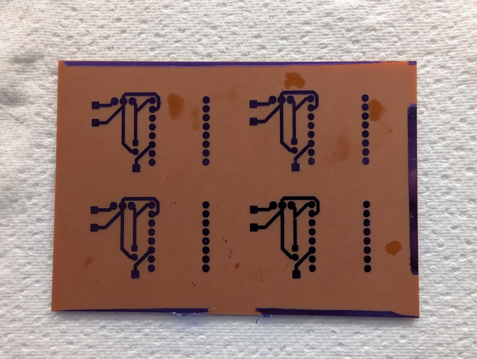
The developer is sodium carbonate decahydrate (washing soda) at 10 g per 500 ml of water. The board goes in and gets agitated, and the unexposed film dissolves away over a minute or two, leaving the hardened resist on the copper only where the artwork let the light through. Stop when just the artwork remains and the clear areas show bright copper. Then put it back under the UV lamp to re-cure: the developed resist is still a little soft, and a second dose of UV hardens it so it survives the etch without lifting at the edges. (The photo below was actually taken after etching, so the areas around the cured resist are already bare fibreglass; straight after developing, the board should be the same purple pattern but with copper everywhere around it.)
7. Etch and strip
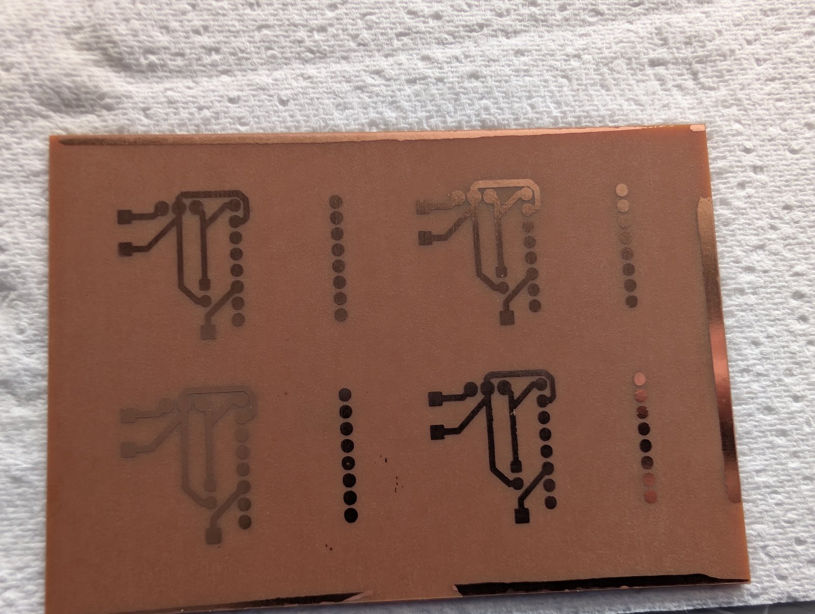
The board is etched in ferric chloride until all the bare copper is gone. Warm etchant and agitation both speed it up considerably; it is worth checking it every few minutes near the end so the traces are not undercut. Once the fibreglass is showing between the traces, rinse the board thoroughly and strip the remaining resist with acetone to reveal the copper underneath.
8. Prep and immersion tin
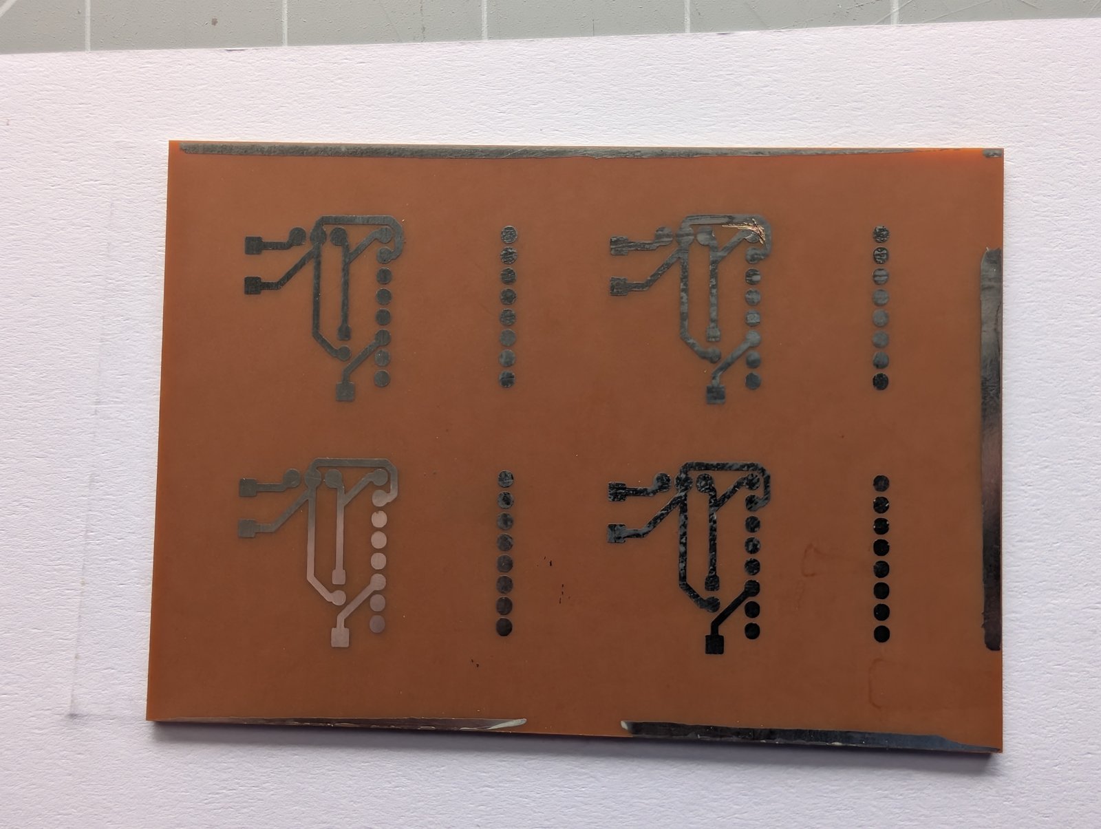
Bare copper tarnishes quickly and solders badly once it has, so the traces get an immersion tin finish. Scrub the board with alcohol and a scourer so the copper is bright, then put it straight into the immersion tin solution. The timing matters: on freshly cleaned copper the tin takes almost instantly, whereas if the board sits around for a while first it goes patchy. The result is a silver, solderable surface that stays that way.
9. Apply the solder mask
The solder mask is a green UV-curable dry film and goes on exactly like the photoresist in step 3: peel, one edge, through the laminator. The difference is that this time there is already a pattern on the board, and the mask artwork (the pads only, printed the same mirrored, doubled way) has to line up with it. Alignment is the critical part of this step; a mask that is off by half a millimetre covers the pads you need to solder to and exposes the traces you want protected, so it is worth taking extra time lining it up against the tinned pads before it goes under the lamp.
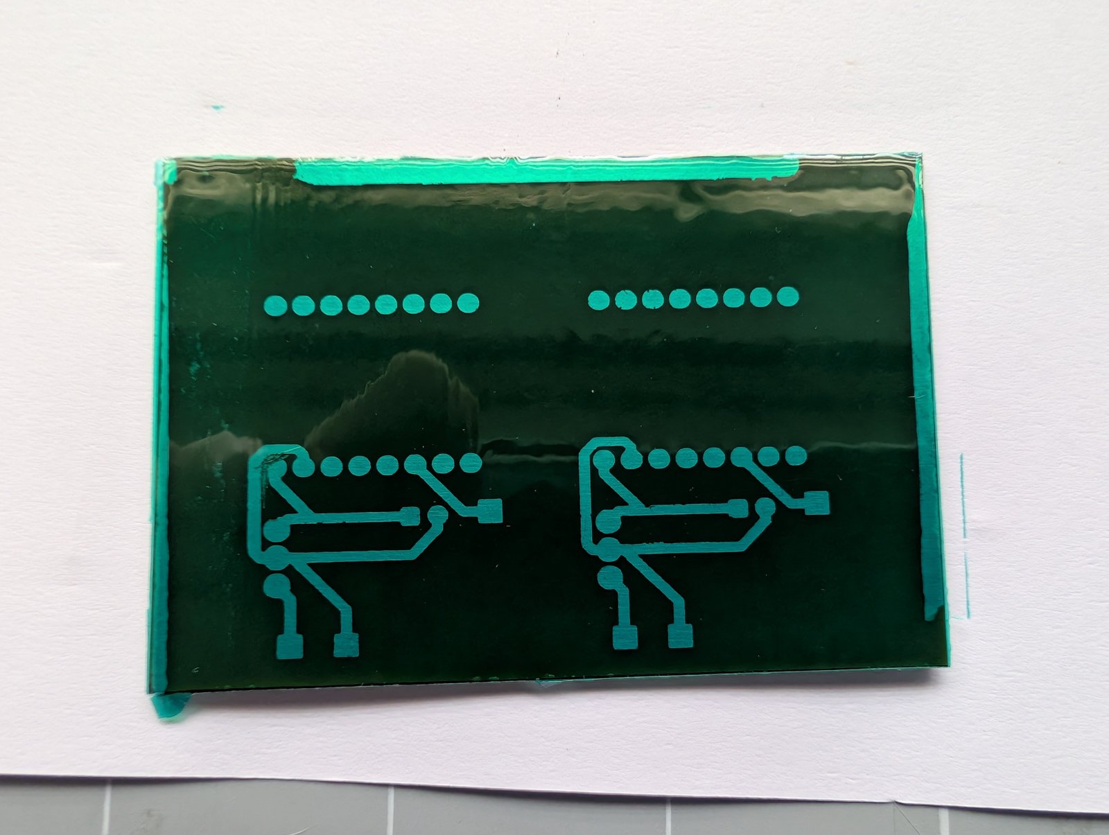
10. Expose and develop the mask
Same again: 10 seconds of UV through the pad artwork, then into the sodium carbonate developer until the pads are clear. The mask artwork is the negative of the photoresist artwork in a sense, since here the areas under the ink are the ones that get washed away, leaving the cured mask everywhere else and open windows over the pads.
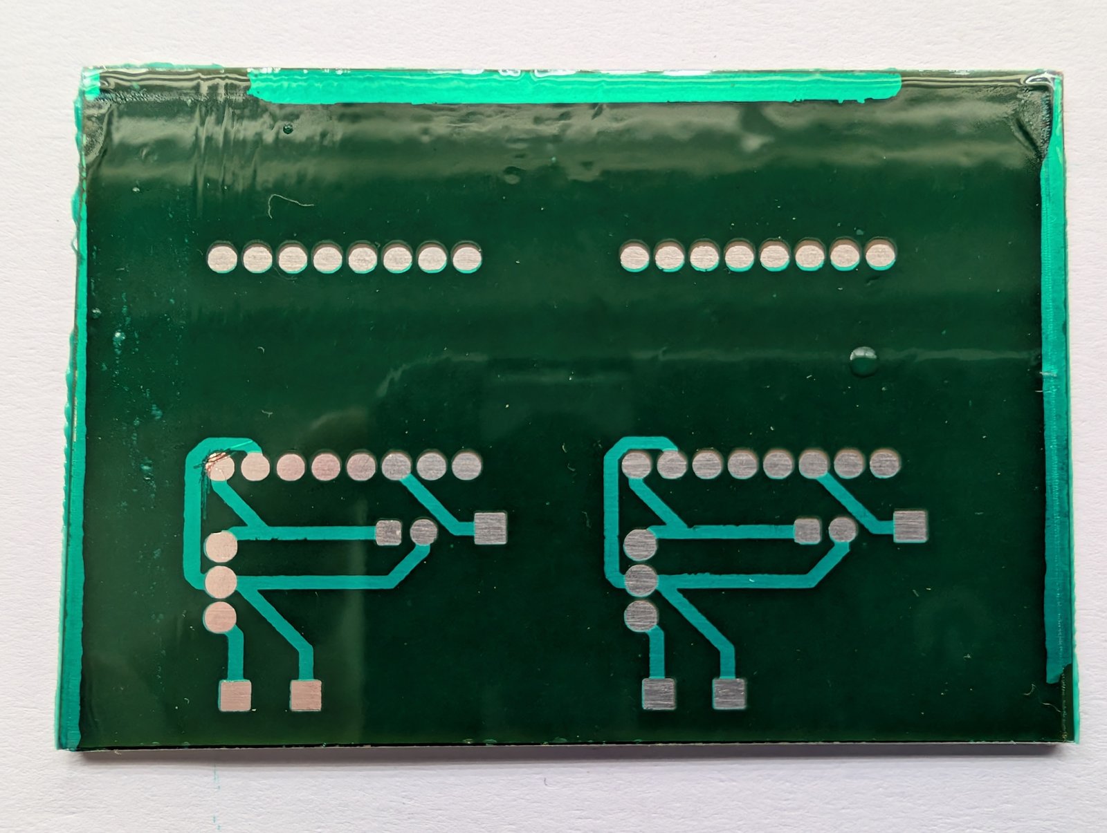
11. Final cure and bake
The mask is cured under the UV lamp for 2 to 3 minutes, much longer than the exposure step because the aim now is to harden all of it rather than to make an image. Then the board is baked in the oven at 150 °C for 60 minutes, which fully hardens the mask so it stands up to the soldering iron. After that it is a finished board: cut the panel apart, drill the holes and it is ready to populate.
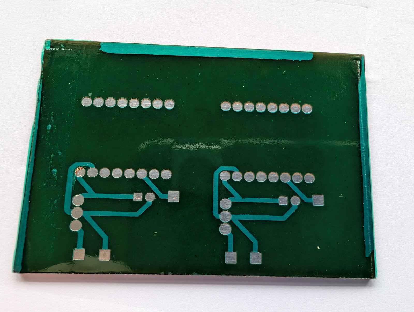
Quick reference
| UV exposure | 10 seconds (photoresist and solder mask) |
|---|---|
| Developer | Sodium carbonate decahydrate, 10 g per 500 ml water |
| Etchant | Ferric chloride |
| Tinning | Immersion tin, immediately after cleaning |
| Final UV cure | 2–3 minutes |
| Oven bake | 150 °C for 60 minutes |
And the four rules that cost me the most boards to learn: artwork mirrored and doubled; one edge, then the laminator; immersion tin straight after cleaning; mind the mask alignment. The poster with all eleven steps on one A4 page is linked below.